We have top-level equipment and advanced process technology, no matter how complex the PCB,
We can quickly provide manufacturing services according to customer requirements.
And has a senior engineering technical team,
according to the customer’s design to make fabrication in a low-cost manner
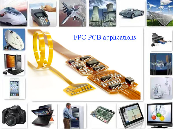
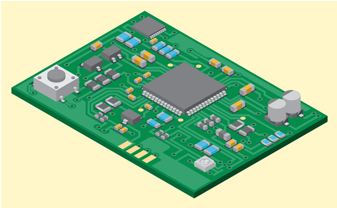
HCH-PCB offers top quality Printing Circuit Boards (PCB) including multi-layer PCB (printed circuit board),
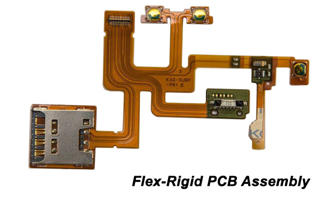
high-level HDI(high density inter-connector), arbitrary-layer PCB and rigid-flexible PCB…etc.
As a base material, HCH-PCB understands the importance of reliable quality of the PCB.
We invest in best equipments and talented team to produce best quality boards.
HCH-PCB manufacturing capabilities are shown in the chart below.
|
Type |
Capability |
|
Scope |
Multilayers(4-70)、HDI(4-48)Flex、Rigid Flex |
|
Double Side |
CEM-3、 FR-4、Rogers RO4233、Bergquist Thermal Clad 4mil–126mil (0.1mm-3.2mm) |
|
Multilayers |
4-70 layers, board thickness 8mil-126mil (0.2mm-3.2mm) |
|
Buried/Blind Via |
4-48 layers, board thickness 10mil-126mil(0.25mm-3.2mm) |
|
HDI |
1+N+1、2+N+2、3+N+3、Any layer |
|
Flex & Rigid-Flex PCB |
1-8layers Flex PCB ,2-12layers Rigid-flex PCB HDI+Rigid-flex PCB |
|
Laminate |
|
|
Soldermask Type(LPI) |
Taiyo、Goo’s、Probimer FPC….. |
|
Peelable Soldermask |
|
|
Carbon ink |
|
|
HASL/Lead Free HASL |
Thickness: 0.5-40um |
|
OSP |
|
|
ENIG (Ni-Au) |
|
|
Electro-bondable Ni-Au |
|
|
Electro-nickel palladium Ni-Au |
Au: 0.015-0.075um Pd 0.02-0.075um Ni:2-6umm |
|
Electro. Hard Gold |
|
|
Thick tin |
|
|
Capability |
Mass Production |
|
Min Mechanical Drill Hole |
0.20mm |
|
Min. Laser Drill Hole |
4mil (0.100mm) |
|
Line Width/Spacing |
2mil/2mil |
|
Max. Panel Size |
21.5″ X 24.5″(546mm X 622mm) |
|
Line Width/Spacing Tolerance |
Non electro coating:+/-5um,Electro coating:+/-10um |
|
PTH Hole Tolerance |
+/-0.002inch(0.050mm) |
|
NPTH Hole Tolerance |
+/-0.002inch(0.050mm) |
|
Hole Location Tolerance |
+/-0.002inch(0.050mm) |
|
Hole to Edge Tolerance |
+/-0.004inch(0.100mm) |
|
Edge to Edge Tolerance |
+/-0.004inch(0.100mm) |
|
Layer to Layer Tolerance |
+/-0.003inch(0.075mm) |
|
Impedance Tolerance |
+/- 10% |
|
Warpage % |
Max≤0.5% |
Technology for HDI PCB
|
ITEM |
Production |
|
Laser Via Drill/Pad |
0.125/0.30 、 0.125/0.38 |
|
Blind Via Drill/Pad |
0.25/0.50 |
|
Line Width/Spacing |
0.10/0.10 |
|
Hole Formation |
CO2 Laser Direct Drill |
|
Build Up Material |
FR4 LDP(LDD); RCC 50 ~100 micron |
|
Cu Thickness on Hole Wall |
Blind Hole: 10um(min) |
|
Aspect Ratio |
0.8 : 1 |
Technology for Flexible PCB
|
Project |
Ability |
|
Roll to roll (one side) |
YES |
|
Roll to roll (double) |
NO |
|
Volume to roll material width mm |
250 |
|
Minimum production size mm |
250×250 |
|
Maximum production size mm |
500×500 |
|
SMT Assembly patch (Yes/No) |
YES |
|
Air Gap capability (Yes/No) |
YES |
|
Production of hard and soft binding plate(Yes/No) |
YES |
|
Max layers(Hard) |
10 |
|
Tallest layer(Soft plate) |
6 |
|
Material Science |
|
|
PI |
YES |
|
PET |
YES |
|
Electrolytic copper |
YES |
|
Rolled Anneal Copper Foil |
YES |
|
PI |
|
|
Covering film alignment tolerance mm |
±0.1 |
|
Minimum covering film mm |
0.175 |
|
Reinforcement |
|
|
PI |
YES |
|
FR-4 |
YES |
|
SUS |
YES |
|
EMI SHIELDING |
|
|
Silver Ink |
YES |
|
Silver Film |
YES |