The optical fiber module is an electronic component used for photoelectric conversion. Simply put, optical signals are
converted into electrical signals, and electrical signals are converted into optical signals, including transmitters,
receivers and electronic functional circuits. Therefore, as long as there is a light signal, there are applications of light
chess pieces. Optical fiber modules are divided into optical receiving modules, optical transmitting modules, optical
transceiver-body modules and optical forwarding modules according to their functions.
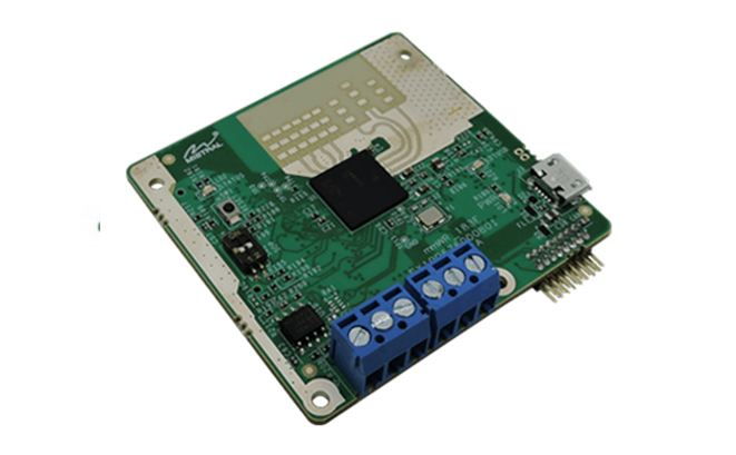
Design method of fiber optical module PCB.
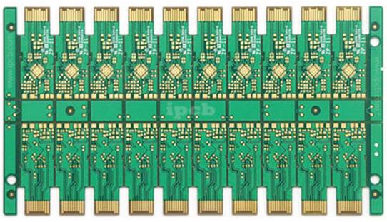
It is recommended for the design of the center mirror symmetrical panel of the miniaturized optical module PCB
It is recommended to place two marking points on the unit board. If the unit board cannot place two marking points,
but at least one marking point can be placed, a marking point without a copper ring can be used. At the same time,
a marking point should be added on the auxiliary side for coordination.
Milling groove + stamp hole design: milling groove width 2mm, stamp hole is non-metallic, recommended hole
distance 1.0mm, aperture 0.5mm,The center of the seal hole should face the PCB of the optical module.
It is recommended that the distance between the center of the seal hole and the edge of the milling groove is not
less than 0.6mm, which can reduce the burrs on the edge of the optical module PCB and avoid interference with
the shell. V-CUT connection: refer to the general requirements of the PCB process design specification.
Milling groove + physical connection: milling groove width 2mm, actual connection width 2-10mm, cloth forbidden
area 1mm,For panel and auxiliary block connection, punching hole + milling groove is the first choice, followed by
real connection + milling groove, V-CUT connection is not recommended.
Note: In the V-CUT connection mode, the milling cutter splitter is not allowed to split the board, and the hob
splitter is used to split the board, the stress is large, and the optical module layout cannot meet the
prohibition requirements.
PCB and FPC welding surface area is not allowed to have any equipment optical device welding hot pressing process:
the hot pressing area is 0.5mm larger than the pressing operation area of the hot pressing head, and the hot pressing
area is equal to or greater than the length of the assembly area + 4mm,Optoelectronic devices fixed with screws:
It is forbidden to lay any devices and non-grounded vias within 1.5mm around the body and bottom and 1.5mm
around the fiber sheath. If it is necessary to arrange non-grounded vias, plug holes must be used to increase the
character oil and green, but non-grounded vias must be prohibited at the bottom of the silk screen.
There is a gap of about 0.25 between the screw hole of the optoelectronic device and the screw, and the tolerance
of the device itself is +0.25. When the tolerance of the device chip is added, a 1.5mm cloth ban is required.
It is forbidden to place vias, test boards and devices around the 1.0mm pads of hand-soldered optical devices.
If a through hole must be arranged, the through hole must be completely blocked with soldermask. The bright
copper area cannot be directly connected to the pad, and there must be a solder mask in the middle.
The minimum width of the solder mask is 3mil, The arrangement distance between optical devices and between
optical devices and electrical components should meet the operating space requirements of manual welding and
maintenance. The pins of optical devices are basically manual welding, so the layout must meet the requirements
of manual welding, otherwise it is easy to hit Parts, causing difficulties in welding and maintenance. In the layout
of the optical component, the fiber exiting part cannot enter the plugging and unplugging area of the fiber
connector, so as not to break the fiber exiting portion of the optical module pigtail when plugging and
unplugging the connector.
For the traces connected to the PCB hot rod reflow soldering pads, the recommended line width is 5-10mil; when a
large area is required for grounding, the lead length d≥50mil,Note: According to the test results, if the length of the
large-area grounding lead is too small, the heat transfer is too fast during hot pressing, and the process parameters
are not easy to control, resulting in poor welding. Therefore, it is recommended that the lead length be greater than
50 mils. Thick and long wiring, connection vias, large area copper foil heat dissipation, resulting in uneven
temperature welding reliability is not consistent.
It is forbidden to design through holes for the non-thermal pads of the device.
ENIG surface treatment is preferred. For hotbar pads, oSP surface treatment is prohibited.
The PCB thickness of SFP and XFP optical modules must be 1.0mm. (The 1.0mm thickness required by SFP and XFP is
specified by the MSA agreement)For pcb technical questions, HCH-PCB’s knowledgeable support team is always available to help you.
You can also request a PCB quotation here.Please contact email sales@hch-pcb.com We will respond very quickly.