High density interconnect PCBs are a way of making more room on your PCB to make them more efficient and allow
for faster transmission. It’s relatively easy for most enterprising companies that are using printed circuit boards to
see how this can benefit them.
High density interconnect (HDI) PCBs represent one of the fastest-growing segments of the PCB market. Because
of its higher circuitry density, the HDI technology can incorporate finer lines and spaces, smaller vias and capture
pads, and higher connection pad densities. A high-density PCB features blind and buried vias and often contains
microvias that are .006 in diameter or even less
Key HDI PCB Benefits
The evolution of PCB HDI technology has given engineers greater design freedom and flexibility than ever before.
Designers using HDI high density interconnect methods now can place more components on both sides of the raw
PCB if desired. In essence, an HDI PCB gives designers more space to work with, while allowing them to place
smaller components even closer together. This means that a high-density interconnect PCB ultimately results in
faster signal transmission along with enhanced signal quality.
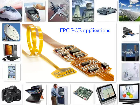
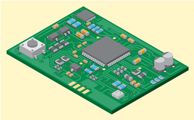
HDI PCB is widely used to reduce the weight and overall dimensions of products, as well as to enhance the electrical
performance of the device. The high-density PCB is regularly found in mobile phones, touch-screen devices, laptop
computers, digital cameras and 4G network communications. The HDI PCB is also prominently featured in medical
devices, as well as various electronic aircraft parts and components. The possibilities for high-density interconnect
PCB technology seem almost limitless.
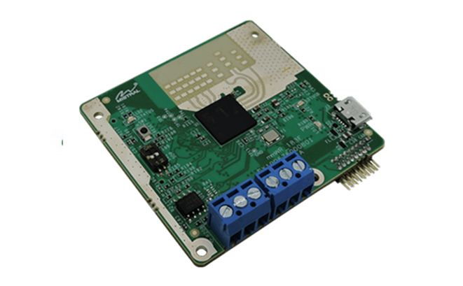
HDI boards are appropriate for a wide range of industries. As mentioned above, you’ll find them in all types of digital
devices, like smartphones and tablets, where miniaturization is key to the effective application of the product. You can
also find high-density interconnect PCBs in automobiles, aircraft and other vehicles that rely on electronics.
One of the most critical areas where the high-density PCB is making huge inroads is in the medical arena. Medical
devices frequently need small packages with high transmission rates that only HDI PCBs can supply. For example,
an implant needs to be small enough to fit in the human body, but any electronics involved in that implant absolutely
must efficiently allow for high-speed signal transmission. Here, the HDI PCB indeed is a godsend. HDI PCBs can also
be useful in other medical equipment, like emergency room monitors, CT scans and much more.
No matter your industry, you’re probably already getting some ideas about how high-density interconnect PCBs can
make the electronics you produce or use even better – get in touch with us PCBCart to discuss it. We’ll let you know
if you’re on the right track and help you decide exactly how beneficial an HDI PCB can be to your industry. Then, you
can determine whether or not to take the next step.
Over the course of a decade in business, HCH-PCB has established a hard-earned reputation for manufacturing PCBs
of the highest quality. Our custom PCB manufacturing capabilities enable you to get the finest quality HDI PCBs at
competitive prices without min order quantity requirement. Our team run design for manufacture check on your
custom PCB file and consult with you to ensure it is ready for manufacturing and that your boards will meet your
performance requirements. We also have an on-site quality control department to verify the finished product meet
your high quality standards.
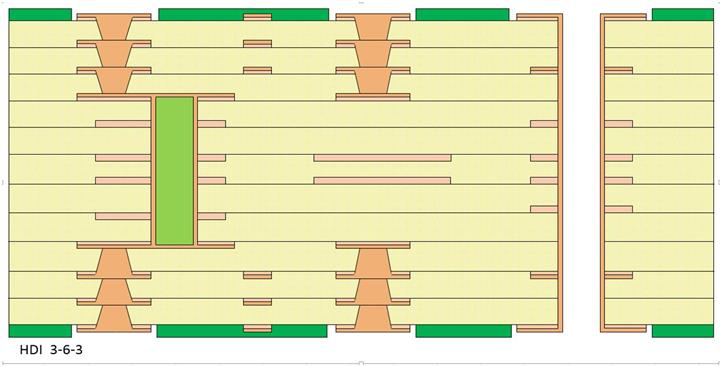
We’re capable of manufacturing HDI PCB up to 56 layers in various structures, check the following table for our
available HDI PCB structures:
| No. | ITEM | Description | Data & Model | ||
| 1 | Material | Brand | SY、ITEQ、KB、NOUYA | ||
| 2 | HDI Construction | 1+N+1、2+N+2、3+N+3、4+N+4、5+N+5、6+N+6、anylayer | |||
| 3 | Construction order | N+N、N+X+N、1+(N+X+N)+1 | |||
| 4 | Layer | 1-56 Layers | |||
| 5 | Min Pattern Width / Spacing | Unit:mil | 2/2 | ||
| 6 | Min Mechanical Hole | Unit:mm | 0.15mm | ||
| 7 | Min Thickness of Core Board | Unit:mil | 2mil | ||
| 8 | Laser Hole | Unit:mm | 0.075mm- 0.1mm | ||
| 9 | Min thickness of PP | Unit:mil | 2mil | ||
| 10 | Max diameter of resin plug hole | Unit:mm | 0.4mm | ||
| 11 | Electroplating to fill holes | Can do it. | |||
| 12 | Electroplating to fill holes size | Unit:mil | 3-5mil | ||
| 13 | hole pile pad/hole pile hole/pad hole(VOP) | mil | Can do it. | ||
| 14 | The distance from the wall of via hole to the | mil | 7mil | ||
| pattern | |||||
| 15 | Laser drilling hole accuracy | mil | 0.025mm | ||
| 16 | Min BGA pad center distance | mil | 0.3mm | ||
| 17 | Min SMT | mil | 0.25mm | ||
| 18 | Plating hole-filling sag | mil | ≤10um | ||
| Technical support or quotation service, please contact. Email: sales@hch-pcb.com Web: www.hch-pcb.com | 1/2 | ||||
| 19 | Back drilled/countersink hole tolerance | mil | ±0.05mm |
| 20 | Through-hole plating penetration capacity | Rate | 16:1 |
| 21 | Blind hole plating penetration capacity | Rate | 1.2:1 |
| 22 | BGA min PAD | Unit:mil | 0.2 |
| 23 | Min Buried Hole(Mechanical Hole) | Unit:mil | 0.2 |
| 24 | Min Buried Hole(Laser Hole) | Unit:mil | 0.1 |
| 25 | Min Blind Hole(Laser Hole) | Unit:mil | 0.1 |
| 26 | Min Blind Hole(Mechanical Hole) | Unit:mil | 0.2 |
| Minimum spacing between laser blind hole | |||
| 27 | and mechanical buried hole | Unit:mil | 0.2 |
| 28 | Min Laser Hole | Unit:mil | 0.10(depth≤55um)、0.13(depth≤100um) |
| 29 | MinBGA pad center distance | Unit:mil | 0.3 |
| 30 | Interlaminar alignment | Unit:mil | ±0.05mm(±0.002″) |
| The distance from the wall of via hole to the pattern | |||