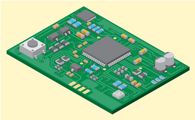
As one type of the most advanced PCB (Printed Circuit Board), IC substrate PCB has exploded in both popularity
and applications together with any layer HDI PCB and flex-rigid PCB, now widely applied in telecommunications
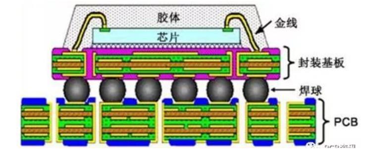
and electronics updates. IC substrate is a kind of substrate used to package bare IC (integrated circuit) chips,
connecting chips and circuit boards.
IC substrate is a type of base board used to package bare IC (integrate circuit) chip. Connecting chip and circuit
board, IC belongs to an intermediate product with the following functions:
Classified by package types
loss, well-performed performance and effective thermal dissipation.
with different functions into one package. As a result, the product can be an optimal solution due to its attributes
including lightness, thinness, shortness and miniaturization. Naturally, since multiple chips are packaged into
one package, this type of substrate doesn’t perform so well in signal interference, thermal dissipation,
fine routing etc.
Classified by material attribute
thermal expansion) is approximately 13 to 17ppm/°C.
or silicon carbide. It features a relatively low CTE which is approximately 6 to 8ppm/°C
Classified by bonding technology
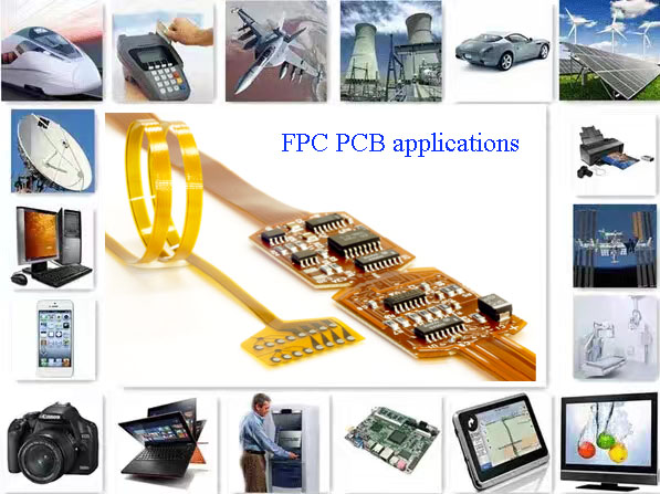
IC substrate PCBs are mainly applied on electronic products with light weight, thinness and advancing functions,
such as smart phones, laptop, tablet PC and network in fields of telecommunications, medical care, industrial control,
aerospace and military.
Rigid PCBs have followed through a series of innovations from multilayer PCB, traditional HDI PCBs,
SLP (substrate-like PCB) to IC substrate PCBs. SLP is just a type of rigid PCBs with similar fabrication process
approximately semiconductor scale.
Compared with standard PCB, IC substrate has to conquer manufacturing difficulties for its implementations of high
performance and advanced functions.
IC substrate is thin and easy to be deformed, which is especially protruding when a board is less than 0.2mm thick.
To overcome this difficulty, breakthroughs have to be made in terms of board shrinking, lamination parameters and
layer positioning system so that substrate warpage and lamination thickness can be effectively controlled.
Microvia technology consists of the following aspects: conformal mask, laser-drilled micro blind via technology and
plated copper filling technology.
can be directly defined through copper openings.
side etching, left gel under via etc.
openness, sinking, copper plating reliability etc.
Patterning and copper plating technology is correlated with the following technological aspects: circuitry
compensation technology and control, fine line fabrication technology, copper plating thickness uniformity control.
Solder mask manufacturing for IC substrate PCB consists of via filling technology, solder mask printing
technology etc. Up to now, IC substrate PCB allows less than 10um for surface height difference and surface
height difference between solder mask and pad should not be over 15 um.
Surface finish for IC substrate PCB should emphasize thickness uniformity and up to now, surface finish that
can be accepted by IC substrate PCB includes ENIG/ENEPIG.
IC substrate PCB calls for inspection equipment that is different from that used for traditional PCB. In addition,
engineers have to be available that are capable of mastering inspection skills on the special equipment.
| No. | Item | Description | Data & Model |
| 1 | Sheng Yi | Core Brand | SI643HU、SI10U、SI09U、SI07U、SI05U |
| 2 | Mitsubishi Gas Chemical | Core Brand | HL832NXA、HL832NS、HL832NSR(LC) |
| 3 | DooSan | Core Brand | DS-7409HGB(S)、DS-7409HGB(LE)、DS-7409HGB(X) |
| 4 | Panasonic | Core Brand | R1515E/R1515H、 |
| 5 | Layer | 1-8layer | |
| 6 | Min pattern size | um | 25 |
| 7 | Min pattern Space | um | 25 |
| 8 | Min Pad | um | 80 |
| 9 | Min BGA Center Space | um | 250 |
| 10 | 2L Min Thickness | um | 80 |
| 11 | 2L Min thickness/core/PP Thickness | um | 80/30 |
| 12 | 4L Min thickness/core/PP Thickness | um | 150/30/20 |
| 13 | 6L Min thickness/core/PP Thickness | um | 210/30/20 |
| 14 | 8L Min thickness/core/PP Thickness | um | 300/30/20 |
| 15 | Soldermask Color | Green, Black | |
| 16 | SM Ink | EG23A、AUS308、AUS320、AUS410 | |
| 14 | Surface treatment | Soft Gold Plating,Hard Gold Plating,ENIG,OSP | |
| 18 | Flatness | um | 5max |
| 19 | Min hole size | um | 100 |
| 20 | Min Laser hole size | um | 50 |
| 21 | Min thickness tolerance | um | 30 |
| 22 | Min PP | um | 25 |
| 23 | Min Core | um | 40 |
| 24 | Minimum Finger Center Distance | um | 65 |
| 25 | Min para-position accuracy | um | 15 |
| 26 | Support Process | Subtraction process, mSAP Process | |
| 27 | Soldermask tolerance | um | 5 |