When talking about printed circuit boards, the terms “PCB schematics” and “PCB designs” are used frequently and interchangeably, but they actually refer to different things. Understanding how they differ is a key to successfully making one, so to help you do that, we’re going to break down the key differences between PCB schematics and PCB designs.
Shenzhen Professional ODM Printed Circuit Board Manufacturer
PCB Schematics vs. PCB Designs
A PCB schematic is a simple two-dimensional circuit design showing the functionality and connectivity between different components. PCB designs, on the other hand, are three-dimensional layouts that indicate those components’ locations once you know your circuit works.
The PCB schematic, then, is the first part of designing a printed circuit board. It’s a pictorial representation, either written or on a computer, that utilizes agreed-upon symbols to describe circuit connections. It also indicates the components that will be used and how they are connected. Anyone should be able to pick up and read the PCB schematic.
Its name aptly describes it: the PCB schematic is a plan, a blueprint. Its concern is not where specifically the components will be located. Instead, the schematic lays out how the PCB will ultimately achieve connectivity and forms a critical part of the planning process.
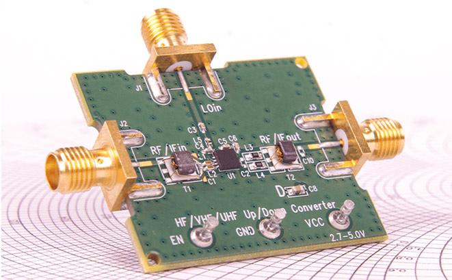
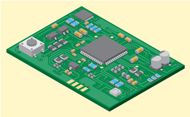
The PCB design does show the locations of the components mentioned above, as well as their connections with copper.
PCB design is the phase that’s concerned with performance. Engineers build the real components on top of the PCB design, allowing them to test whether the device works or not. We mentioned before that anyone should be able to understand a PCB schematic, but the functionality is not readily understood by looking at the prototype.
Once both of these phases have been completed and you’re satisfied with the performance of your PCB, printed board circuit manufacturers can help you bring your device to life.
Now that you have a broad overview of the differences between the two, let’s take a closer look at the elements of PCB schematics. As we mentioned, all the connections are visible, but there are some things to keep in mind:
* To be able to see the connections clearly, they are not created to scale; on the PCB design, they may be quite close to one another
* Some connections might cross one another, which can’t happen on the physical version
* Some connections might be on opposing sides of the layout with markings indicating that they are linked
* This PCB “blueprint” may be represented on one page, two pages, or even several pages–as many as it takes to fully depict everything that needs to be included in the design
One final thing to note is that more complicated schematics may be grouped by function to aid readability. Arranging connections in this manner is something that doesn’t happen in the next stage, and schematics often don’t match up to the final design on the 3-D model.
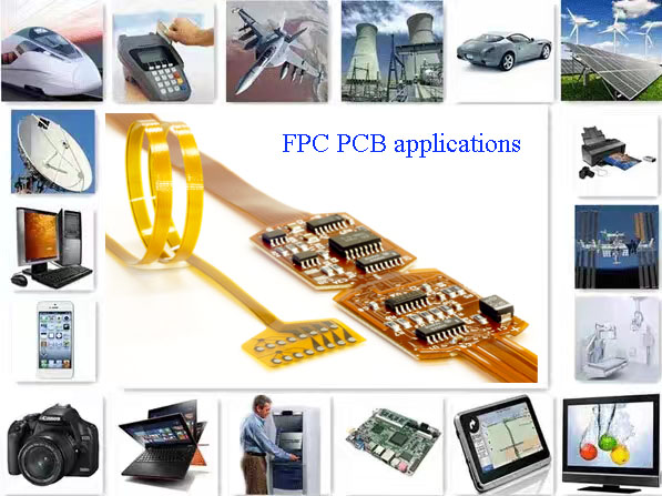
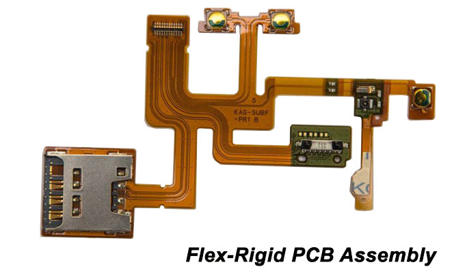
Now it’s time to take a more in-depth look at PCB designs elements. At this stage, we move from written blueprints to a physical representation that is constructed using laminate or ceramic material. Some more complicated applications require the use of flexible PCB when exceptionally tight space is a concern.
The elements of PCB designs follow the blueprint that the schematics process has laid out, but, as we’ve mentioned, look very distinct visually. We’ve already talked about what the PCB schematics look like, but what differences can we observe in the design?
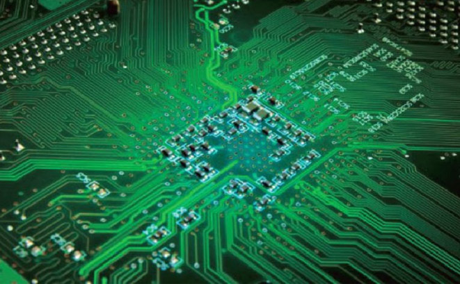
When we talk about PCB designs, we’re talking about a 3-D model that includes the printed circuit board and the design files. They can be single or multiple layers, though they are most commonly two layers.
Though these terms are often used interchangeably, as you can see, PCB schematic VS PCB designs refer to two separate, distinct processes in the creation of a printed circuit board. You can’t have PCB designs without first creating PCB schematics that map out the process, and your PCB design is an integral part of bringing your electronic creation to life.